Technical Documents
Specifications
Brand
Texas InstrumentsLogic Family
LVC
Product Type
Buffer & Line Driver
Logic Function
Buffer
Schmitt Trigger Input
Yes
Input Type
CMOS
Mount Type
Surface
Output Type
CMOS
Minimum Supply Voltage
1.65V
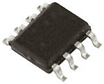
Package Type
US
Pin Count
8
Maximum Supply Voltage
5.5V
Minimum Operating Temperature
-40°C
Maximum High Level Output Current
-32mA
Maximum Low Level Output Current
32mA
Maximum Operating Temperature
125°C
Height
0.8mm
Length
2.15mm
Standards/Approvals
RoHS
Series
SN74LVC2G125
Automotive Standard
No
Product Details
Ideate. Create. Collaborate
JOIN FOR FREE
No hidden fees!


Stock information temporarily unavailable.
€ 515.08
€ 0.172 Each (On a Reel of 3000) (Exc. VAT)
3000
€ 515.08
€ 0.172 Each (On a Reel of 3000) (Exc. VAT)
Stock information temporarily unavailable.
3000
Ideate. Create. Collaborate
JOIN FOR FREE
No hidden fees!
Technical Documents
Specifications
Brand
Texas InstrumentsLogic Family
LVC
Product Type
Buffer & Line Driver
Logic Function
Buffer
Schmitt Trigger Input
Yes
Input Type
CMOS
Mount Type
Surface
Output Type
CMOS
Minimum Supply Voltage
1.65V
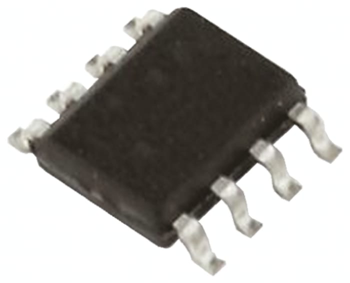
Package Type
US
Pin Count
8
Maximum Supply Voltage
5.5V
Minimum Operating Temperature
-40°C
Maximum High Level Output Current
-32mA
Maximum Low Level Output Current
32mA
Maximum Operating Temperature
125°C
Height
0.8mm
Length
2.15mm
Standards/Approvals
RoHS
Series
SN74LVC2G125
Automotive Standard
No
Product Details
Ideate. Create. Collaborate
JOIN FOR FREE
No hidden fees!