Technical Documents
Specifications
Brand
NexperiaPackage Type
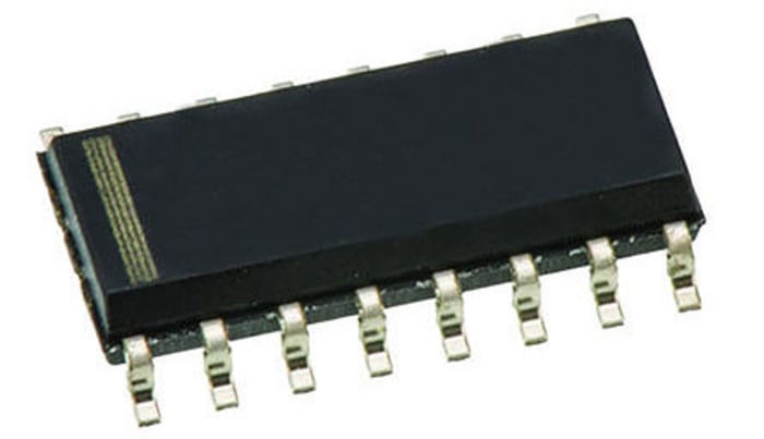
SOIC
Logic Function
Shift Register
Number of Stages
8
Logic Family
HC
Mounting Type
Surface Mount
Operation Mode
Serial to Serial, Parallel
Number Of Elements
1
Pin Count
16
Minimum Operating Supply Voltage
2 V
Maximum Operating Supply Voltage
6 V
Dimensions
10 x 4 x 1.45mm
Minimum Operating Temperature
-40 °C
Triggering Type
Positive Edge
Maximum Operating Temperature
125 °C
Direction Type
Uni-Directional
Product Details
The 74HC4094, 74HCT4094 is an 8-bit serial-in/serial or parallel-out shift register with a storage register and 3-state outputs. Both the shift and storage register have separate clocks. The device features a serial input (D) and two serial outputs (QS1 and QS2) to enable cascading. Data is shifted on the LOW-to-HIGH transitions of the CP input. Data is available at QS1 on the LOW-to-HIGH transitions of the CP input to allow cascading when clock edges are fast. The same data is available at QS2 on the next HIGH-to-LOW transition of the CP input to allow cascading when clock edges are slow. The data in the shift register is transferred to the storage register when the STR input is HIGH. Data in the storage register appears at the outputs whenever the output enable input (OE) is HIGH.

Ideate. Create. Collaborate
JOIN FOR FREE
No hidden fees!



Stock information temporarily unavailable.
Price on asking
Standard
1
Price on asking
Stock information temporarily unavailable.
Standard
1
Ideate. Create. Collaborate
JOIN FOR FREE
No hidden fees!
Technical Documents
Specifications
Brand
NexperiaPackage Type
SOIC
Logic Function
Shift Register
Number of Stages
8
Logic Family
HC
Mounting Type
Surface Mount
Operation Mode
Serial to Serial, Parallel
Number Of Elements
1
Pin Count
16
Minimum Operating Supply Voltage
2 V
Maximum Operating Supply Voltage
6 V
Dimensions
10 x 4 x 1.45mm
Minimum Operating Temperature
-40 °C
Triggering Type
Positive Edge
Maximum Operating Temperature
125 °C
Direction Type
Uni-Directional
Product Details
The 74HC4094, 74HCT4094 is an 8-bit serial-in/serial or parallel-out shift register with a storage register and 3-state outputs. Both the shift and storage register have separate clocks. The device features a serial input (D) and two serial outputs (QS1 and QS2) to enable cascading. Data is shifted on the LOW-to-HIGH transitions of the CP input. Data is available at QS1 on the LOW-to-HIGH transitions of the CP input to allow cascading when clock edges are fast. The same data is available at QS2 on the next HIGH-to-LOW transition of the CP input to allow cascading when clock edges are slow. The data in the shift register is transferred to the storage register when the STR input is HIGH. Data in the storage register appears at the outputs whenever the output enable input (OE) is HIGH.
Ideate. Create. Collaborate
JOIN FOR FREE
No hidden fees!